Dimensions of the 0402 Package: Size, Tolerances, and PCB Design
Explore the dimensions of the 0402 package, including nominal size, tolerances, and their impact on PCB land patterns, with guidance from What Dimensions.

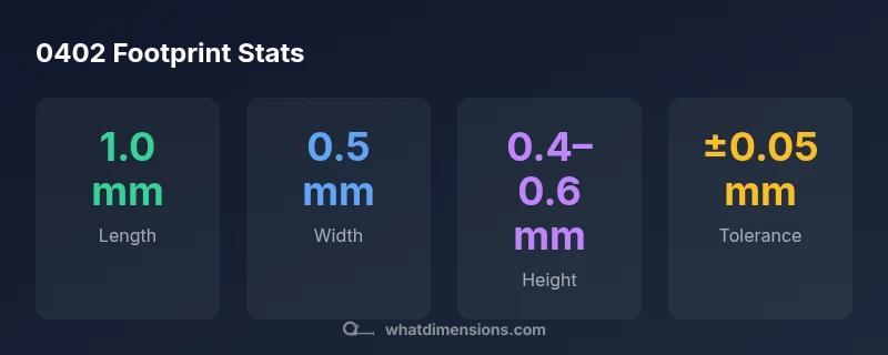
The dimensions of the 0402 package are about 1.0 mm long by 0.5 mm wide, which corresponds to the common 0402 footprint for SMD resistors and capacitors. In imperial terms, that's 0.04 inches by 0.02 inches. Tolerances typically allow ±0.05 mm in length and width, with height around 0.4–0.6 mm depending on manufacturer. Always verify actual part drawings. This footprint is widely used in high-density boards and requires careful layout.
What the 0402 Package Is and Why Size Matters
The 0402 package is one of the smallest widely used surface-mount device footprints for resistors, capacitors, and other passive components. Its compact size (about 1.0 mm long by 0.5 mm wide) enables high circuit densities and compact boards, but also imposes tighter tolerances, stricter land patterns, and more stringent manufacturing controls. For designers, the exact dimensions influence solder paste deposition, component placement, and rework feasibility. In metal-oxide varistors or ceramic caps, the footprint must align with the resistor/capacitor's body to ensure reliable solder joints and consistent thermal performance. This article (based on What Dimensions Analysis, 2026) provides precise figures and practical guidance for engineers, students, and hobbyists who need to ensure fit, clearance, and manufacturability in real boards.
Nominal Dimensions and Common Tolerances
Nominal dimensions of the 0402 package are widely specified as 1.0 mm by 0.5 mm. In imperial units, the footprint is commonly cited as 0.04 in by 0.02 in. However, manufacturers may define small tolerances depending on molding and plating processes. Typical tolerances are around ±0.05 mm for length and width, with height varying from about 0.4 to 0.6 mm across parts and vendors. The result is an effective footprint envelope that must fit your PCB land patterns and stencil guidelines. The key takeaway is to design to the worst-case boundary rather than the nominal figure, and to verify with actual part drawings from suppliers. What Dimensions stresses cross-checking data sheets to avoid mismatch.
Height, Pads, and Land Patterns: How Size Affects PCB Design
The tiny dimensions of the 0402 package have a direct impact on land patterns and pad geometry. Because the body is only 1.0 mm by 0.5 mm, the solderable land must be precise to avoid tombstoning, skew, or insufficient solder fillets. Designers should rely on IPC-7351 (land patterns) and the specific component manufacturer’s footprint recommendations, then validate with CAD tools and paste deposition simulations. Mask expansions and stencil apertures must reflect both nominal dimensions and tolerances to ensure consistent solder joints across lots. What Dimensions notes that even small deviations in the land pattern can ripple into yield losses on dense boards.
Measurement and Verification Techniques
Measuring a 0402 part demands careful technique due to its small size. Calipers can give quick checks of length and width, but optical comparators or high-magnification digital microscopes deliver more reliable results for verification against drawings. A simple best practice is to measure multiple samples from a production batch and compare against supplier drawings and IPC tolerances. For hobbyists, a calibrated magnifier and a ruler with fine gradations can still provide meaningful checks before committing to board fabrication. What Dimensions emphasizes relying on official drawings and cross-checking with your board house’s recommended footprints.
Practical Design Tips for Engineers and Hobbyists
- Always start from a vendor-supplied footprint or IPC-7251/IPC-7351 pattern tailored to 0402 components. - Use solder mask clearance to protect pads without risking tombstoning. - When in doubt, order a small test panel with multiple footprints to validate assembly yield. - Consider stencil thickness and paste volume for such tiny components, as excessive paste can cause bridges. - Keep component spacing and routing generous enough near the 0402 area to avoid misalignment during rework. What Dimensions recommends validating footprints with real-world prototypes before mass production.
Manufacturing and Quality Considerations
During reflow, the tiny 0402 body thickness can influence heat transfer and solder quality. Ensure your paste deposition and board temperatures meet the component’s limits, and confirm that the land pattern tolerances are aligned with the manufacturer’s datasheet. Shift in board flex or anchor points can alter joint geometry, so it is wise to include margin in critical nets. The vendor’s drawings should be the primary reference, with IPC standards providing secondary guidance. What Dimensions highlights that tolerances aren’t just numbers; they’re guardrails for reliable electronics.
How to Maintain Consistency Across Vendors
Different manufacturers may slightly vary the body height and land pattern recommendations for 0402 parts. Maintain consistency by using the same footprint family across suppliers and performing cross-verification with each lot. Keep a library of validated footprints and document any deviations observed during incoming inspection. For critical assemblies, consider a supplier-fit program that runs dimensional checks on a sample of parts from each batch to prevent surprises on the line.
Summary: Why Care About the Dimensions of 0402 Package
Tiny footprints drive density, not just aesthetics. The dimensions of the 0402 package influence board real estate, solder reliability, and manufacturability. By aligning your land patterns with official drawings and following IPC guidance, you can reduce rework and improve board-level performance. The What Dimensions team encourages engineers to treat these dimensions as dynamic—subject to vendor variation and manufacturing realities—and to verify with up-to-date data sheets.
0402 footprint dimensions overview
| Dimension | Nominal | Notes |
|---|---|---|
| Length (L) | 1.0 mm | ±0.05 mm tolerance |
| Width (W) | 0.5 mm | ±0.05 mm tolerance |
| Height (H) | 0.4-0.6 mm | Varies by vendor |
| Imperial (L×W) | 0.04 in × 0.02 in | Metric-to-imperial conversion |
Quick Answers
What are the standard dimensions of the 0402 package?
The 0402 package has nominal dimensions of 1.0 mm by 0.5 mm. Always consult the supplier’s drawings for tolerances and height.
The standard 0402 footprint is 1.0 by 0.5 millimeters; check the supplier drawings for exact tolerances.
How tight are the tolerances for the 0402 footprint?
Typical tolerances are around ±0.05 mm for length and width; height can vary by vendor. Use official drawings for exact values.
Tolerances are typically about plus or minus five hundredths of a millimeter for length and width.
Why does height variation matter for 0402 assemblies?
Height variations affect stacking, clearance, and solder fillets, especially in dense boards. Verify against drawings and use consistent footprints.
Height varies by part and vendor; it can affect clearance in dense boards, so verify with drawings.
When should I use a 0402 footprint vs a larger size?
Choose 0402 for high-density layouts when space is critical, but ensure manufacturability and reliable rework by testing early footprints.
Pick 0402 for density, but prototype first to ensure manufacturability.
Where can I find official drawings for 0402 footprints?
Start with supplier datasheets and IPC standards; cross-check with the device manufacturer’s footprint recommendations.
Check supplier datasheets and IPC standards for official drawings.
“Precise dimensions drive reliable solder joints and high-yield assemblies for tiny footprints like the 0402. Rely on manufacturer drawings and IPC guidelines to anchor your designs.”
Main Points
- Design to worst-case tolerances for 0402 components.
- Always use manufacturer drawings and IPC footprints.
- Validate with real-world prototypes before production.
- Consider paste, stencil, and mask clearances in tiny footprints.
- Cross-check dimensions across suppliers to avoid assembly issues.