Dimensions of 0402 Capacitor: Footprint, Tolerances, and Board Design
An in-depth look at the dimensions of the 0402 capacitor: footprint (1.0 x 0.5 mm), height, tolerances, and how sizing impacts PCB land patterns and soldering.

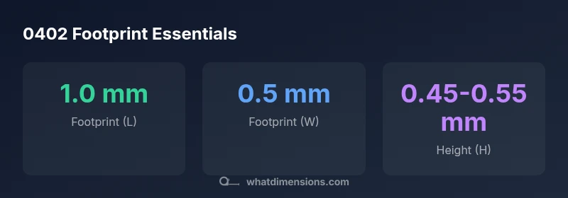
The standard footprint for a 0402 capacitor is 1.0 mm by 0.5 mm, with a typical height of about 0.45–0.55 mm. This defining size class is the smallest common SMD package, influencing PCB land patterns, soldering tolerances, and assembly practices. For precise projects, consult each supplier's datasheet.
Understanding the dimensions of 0402 capacitor and why they matter
The dimensions of the 0402 capacitor define its footprint on a printed circuit board and influence how components are placed, soldered, and inspected. In practice, the size determines land-pattern guidelines, pick-and-place tolerances, and even the reliability of reflow soldering. The 0402 code corresponds to a footprint around 1.0 mm by 0.5 mm in the metric system, a standard widely used in consumer electronics, wearables, and compact PCBs. According to What Dimensions, standardized metrics help designers create reusable patterns that fit across vendors while maintaining solderability and electrical performance. The What Dimensions team found that engineers often underestimate the impact of tiny dimensional differences: even a tenth of a millimeter in L or W can shift pad geometry enough to alter solder fillet formation or part alignment during automated assembly. Therefore, a deliberate approach to reading datasheets, selecting the right tolerance class, and validating footprints on actual boards is essential for production yield and long-term reliability.
Footprint and physical geometry explained
The 0402 capacitor footprint is defined by three critical measurements: length (L), width (W), and height (H). L and W determine pad shape and spacing, while H affects stencil design, solder paste deposition, and thermal mass during reflow. The metric footprint of 1.0 x 0.5 mm is widely adopted because it balances mechanical stability with the need to conserve board real estate. Designers should refer to IPC/JEDEC guidelines and individual supplier datasheets to confirm the exact L x W tolerance and height range for the part family they select. Even within the same code, vendors may offer tight or looser tolerances depending on dielectric formulation and plating processes, which can subtly affect assembly yield.
Imperial vs metric sizing and standardization
Electronic component sizing uses both metric and imperial references. The 0402 code originates from the imperial system (0.04 x 0.02 inches) and maps to 1.0 x 0.5 mm in metric terms. This duality matters for international supply chains, as land patterns in different CAD libraries may show dimensions in either unit. Standardization efforts by IPC and major manufacturers aim to keep these numbers consistent, but real-world variability exists. Always align your PCB library footprints with the specific supplier’s datasheet and your design rules to ensure proper fit and reliable solder joints.
Tolerances and manufacturing variability
Manufacturing tolerances for an SMD footprint like 0402 vary by supplier, material, and process controls. In practice, L and W tolerances are typically discussed in datasheets as a range (for example, ±0.05 mm), while height tolerances depend on dielectric material and construction. Designers should plan for small deviations during SMT soldering, which can influence fillet formation and wetting. When tight assembly tolerances are required, select vendors that publish tighter tolerance classes and validate footprints with test boards under your normal reflow profiles. What Dimensions recommends reviewing datasheets and, if possible, ordering samples to verify fit on your production boards.
PCB land patterns and soldering considerations
A precise land-pattern design is essential for 0402 components. Pads should accommodate pad-to-pad spacing, allow adequate solder paste, and provide reliable solder joint geometry under all reflow conditions. Consider stencil thickness, paste volume, and solder paste spread to prevent tombstoning or insufficient fillet formation. Also factor inspection methods (AOI/AXI vs. microscopy) and automated pick-and-place tolerances, which can be sensitive to minute changes in L and W. Using IPC guidelines for small packages and validating with prototype boards helps minimize yield losses.
Measuring and verifying 0402 dimensions in practice
Accurate measurement of 0402 dimensions requires calibrated instruments. Use calipers or optical inspection tools to verify L, W, and H against the supplier’s datasheet. For mass production, coordinate with the PCB fab and assembly house to confirm land-pattern tolerances and reflow profiles. If you need to compare across vendors, build a small data set that shows different vendors’ nominal footprints and their published tolerances, then test these footprints in your actual board layout and assembly flow.
Choosing materials and reliability considerations for 0402 footprints
Dielectric material, termination plating, and solder alloy choices influence the effective height and tolerances of a 0402 capacitor. In practice, thicker terminations or higher-K dielectrics can slightly alter overall package height, impacting clearance in densely packed boards. Designers should select capacitor series whose datasheets clearly specify dimensions, tolerances, and allowable bending moments during reflow. Reliability concerns—such as thermal cycling and moisture sensitivity—may also vary with footprint geometry, so consider environmental scenarios when selecting a part family.
Practical design tips and common mistakes to avoid
Avoid assuming that all 0402 parts are identical. Cross-check multiple vendor datasheets, confirm the exact L x W x H, and verify with prototype boards before committing to a large build. Keep clear notes on your PCB library about which tolerance class you’re using and ensure your DFM checks flag any part-variation risks. Finally, document your design intent for the footprint in the BOM so future designers can reuse a verified pattern without re-deriving it.
Common SMD capacitor footprints for reference
| Size (code) | Footprint (L x W) | Typical height (H) |
|---|---|---|
| 0402 | 1.0 x 0.5 | 0.45-0.55 |
| 0603 | 1.6 x 0.8 | 0.55-0.65 |
| 0201 | 0.6 x 0.3 | 0.45-0.50 |
Quick Answers
What does 0402 mean in capacitor sizing?
0402 is a size code used in SMD components. It corresponds to a footprint of approximately 1.0 x 0.5 mm in metric terms and 0.04 x 0.02 inches in imperial terms. This code helps standardize land patterns and assembly practices.
0402 is a size code for very small SMD capacitors; it maps to roughly 1.0 by 0.5 millimeters.
Are 0402 dimensions standardized globally?
Dimensions are standardized to a large extent by IPC size codes, but there can be vendor-specific tolerances. Always consult the supplier datasheet and align footprints across your PCB libraries.
There is a global standard, but check each vendor’s datasheet for exact tolerances.
How much can height vary for 0402 capacitors?
Height can vary by manufacturer, but typical ranges fall within roughly 0.45 to 0.55 mm. Verify the exact height range in the specific part’s datasheet.
Height usually lies around 0.45 to 0.55 mm, but check the datasheet for the part you’re using.
Can I use 0402 capacitors in higher-frequency designs?
Yes, 0402 capacitors are used in many high-frequency applications, but dielectric type, voltage rating, and package tolerances influence parasitics. Choose parts with appropriate dielectric and verify with your RF design tools.
0402s can be used in many frequencies; pick the right dielectric and verify with your design tools.
What is the impact of 0402 dimensions on PCB land patterns?
Small changes in L and W change pad size and spacing, affecting solder paste and joint quality. Use IPC-7351 guidelines and validate footprints with prototypes.
Tiny size changes alter pads and solder behavior; validate footprints with samples.
What tools can verify 0402 dimensions during assembly?
Use calipers, optical inspection, and cross-check vendor datasheets. For mass production, fixture-based QA and AOI can help catch dimensional deviations.
Calipers and AOI help verify 0402 dimensions in production.
“Precise sizing matters for reliable assembly; even small deviations in the 0402 footprint can affect solder flow and joint quality.”
Main Points
- Understand the 1.0 x 0.5 mm footprint for 0402 capacitors.
- Check datasheets for exact tolerances and height ranges.
- Design land patterns using IPC guidelines and vendor specs.
- Verify footprints with prototypes to ensure reliable soldering.