Dimensions of 0603 Package: A Precise SMD Size Reference
Explore the exact dimensions of the 0603 package, including nominal size, imperial equivalents, tolerances, and footprint considerations for reliable PCB design.

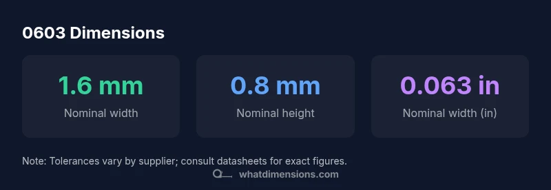
The dimensions of the 0603 package are a nominal 1.6 mm by 0.8 mm (0.063 in by 0.031 in) for SMD resistors and capacitors. In practice, factory tolerances vary by supplier and part, so always verify against the datasheet and IPC footprint guidelines. This size balances compact boards with reliable solder joints, a core concern for high-density designs.
What the 0603 package represents
The 0603 package refers to a common surface-mount device (SMD) size used for resistors, capacitors, and inductors. Its name derives from imperial measurements: 0.06 inches by 0.03 inches, or 1.6 mm by 0.8 mm in metric terms. In electronics manufacturing, this size offers a balance between board density and solderability, making it a ubiquity across consumer gadgets and industrial equipment. According to What Dimensions, the 0603 family is favored for projects where space is tight but lead-free reflow reliability must remain high. Engineers often start with the nominal size and then adjust footprints to accommodate manufacturing tolerances and assembly equipment. The 0603 package’s small footprint supports multi-layer boards, but it also requires precise land patterns and careful handling during automated assembly. Understanding these basic dimensions is the foundation for making informed choices about components, board layout, and inspection strategies.
Nominal dimensions in metric and imperial
The 0603 size is defined as a nominal 1.6 mm × 0.8 mm footprint, which corresponds to about 0.063 inches × 0.031 inches in the imperial system. Designers often rely on both units to ensure compatibility across suppliers and manufacturing lines. While the nominal figures are widely accepted, real parts can deviate slightly due to tolerances and process variations. For practical PCB work, it is essential to cross-check both metric and imperial values on the component datasheet and compare them to your footprint library. This cross-check helps prevent misfits during automated assembly and improves first-pass yield on dense boards.
Tolerances and manufacturing variation
Tolerances for the 0603 package are not standardized to a single value across all manufacturers. They depend on the part type (resistor, capacitor, inductor) and the supplier’s fabrication process. In practice, you should treat the nominal 1.6 × 0.8 mm as a guide and rely on the datasheet for exact tolerances. Footprint libraries should include a small clearance to accommodate minor dimensional drift during solder paste deposition and reflow. As parts move through the supply chain, dimensional variation can accumulate, which is why IPC footprint guidelines and supplier specifications matter greatly for high-density designs.
How 0603 compares to nearby sizes
0603 sits between smaller 0402 and larger 0805 families. The 0402 package is typically around 1.0 × 0.5 mm, providing even higher board density but harsher tolerances, while the 0805 is roughly 2.0 × 1.25 mm, offering easier handling and soldering. This relative sizing helps engineers make trade-offs between density, robustness, and assembly yield. When migrating designs from larger sizes, verify that the land pattern and soldermask clearances scale appropriately to avoid tombstoning or bridging in tight regions.
Footprint and PCB design considerations
Footprint design for the 0603 package should align with IPC-7351 standards and be validated against the actual component series you intend to use. Pad length and spacing should accommodate the body’s dimensions plus a small tolerance buffer. Use a conservative courtyard and ensure adequate solder mask relief so that paste does not wick away or smear the component. For high-density boards, consider fiducials and inspection features to help automated optical inspection (AOI) verify correct placement. Always maintain a consistent process for reflow profiles to minimize misalignment and volume loss.
Manufacturing considerations and assembly
During assembly, the 0603 package benefits from well-controlled paste deposition and a stable reflow profile. Sticky issues include misalignment on ultra-dense boards and tombstoning in resistive networks. To mitigate these risks, verify the footprint against multiple supplier footprints, maintain clearances for tolerances, and align pick-and-place parameters with the actual component sizes. In a production setting, the combination of precise dimensions and reliable soldering directly influences yields and board reliability.
Practical verification techniques
Physically verifying a 0603 component involves both measurement and visual inspection. Use a caliper or optical comparator to confirm that the component’s body length and width are close to 1.6 mm and 0.8 mm, respectively. Cross-check with the PCB footprint in your CAD library and with an on-board AOI inspection step. In prototyping, create a small test coupon with a 0603 footprint and run a quick through-hole or surface-mount reflow experiment to ensure the footprint behaves as expected under your soldering process.
Common pitfalls and design tips
- Do not rely solely on nominal sizes; always confirm tolerances with the datasheet.
- Ensure footprints have sufficient clearance to accommodate solder paste and solder mask.
- When routing fine-pine traces near 0603 components, allow for castellated spacing to prevent shorts.
- Use IPC-7351 or vendor-provided footprints to ensure consistency across libraries.
- Validate footprints across multiple suppliers to account for manufacturing variation.
Sourcing reliable dimensions and standards
Always compare component datasheets, footprint libraries, and IPC standard recommendations to ensure dimensional accuracy. For educational purposes, refer to industry standards and published documentation from recognized authorities to understand how dimensions are defined and listed. This reduces the risk of mismatches between real parts and your PCB footprints and supports better yield during production.
Dimensional references for the 0603 package
| Item | Description | Value | Notes |
|---|---|---|---|
| Nominal size (mm) | Physical body size | 1.6 × 0.8 | Standard SMD package size for 0603 |
| Nominal size (in) | Imperial equivalent | 0.063 × 0.031 | Converted from metric; verify on datasheet |
| Tolerance | Dimensional tolerance | varies by supplier | Refer to datasheet/IPC footprint |
| Common uses | Applications | Resistors, capacitors, inductors | Widely used in compact PCBs |
Quick Answers
What does the '0603' designation mean in SMD packages?
The '0603' designation refers to the package’s nominal size in inches (0.06 by 0.03) or millimeters (about 1.6 × 0.8). It describes a standard surface-mount form factor used for resistors, capacitors, and inductors.
0603 is a standard small SMD size used for many components.
What is the exact size of a 0603 package?
Nominally 1.6 mm by 0.8 mm (0.063 in by 0.031 in). Exact figures vary by supplier and part type, so always consult the datasheet for the specific component.
It’s 1.6 by 0.8 millimeters, but check the datasheet for exact figures.
Do tolerances vary for 0603 parts?
Yes. Tolerances depend on the manufacturer and part type. Always reference the datasheet and the footprint library to determine the allowable deviation for your design.
Tolerances vary by manufacturer, so check the datasheet.
How should I choose a footprint for 0603 on a PCB?
Start with IPC-7351 guidelines and use supply-provided footprints when possible. Validate with prototypes and AOI to ensure solder joints and clearances are reliable.
Use IPC footprints and verify with prototypes.
Where can I find reliable dimensions for 0603 components?
Consult component datasheets, IPC standard documents, and trusted footprint libraries. Cross-check multiple sources to ensure consistency across batches.
Check datasheets and IPC standards.
“Precise size knowledge of the 0603 dimensions directly improves footprint reliability and assembly yield.”
Main Points
- Confirm the nominal 1.6 × 0.8 mm size for the 0603 package.
- Cross-check metric and imperial dimensions on the datasheet.
- Expect variation in tolerances by supplier; use IPC footprints.
- Always verify footprints with the part family and supplier data.
- Leverage IPC-7351 guidelines for reliable land patterns.